Smaller, faster and more efficient modulator sets to revolutionize optoelectronic industry
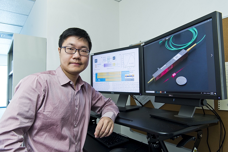
A research team comprising members from City University of Hong Kong (CityU), Harvard University and renowned information technologies laboratory - Nokia Bell Labs - has successfully fabricated a tiny on-chip lithium niobate modulator, an essential component for the optoelectronic industry. The modulator is smaller, more efficient with faster data transmission and costs less. The technology is set to revolutionise the industry.
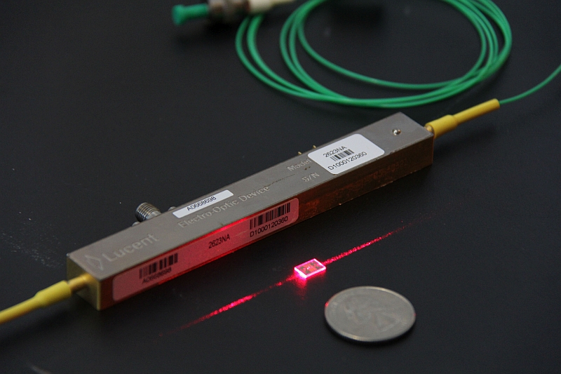
The electro-optic modulator produced in this breakthrough research is only 1 to 2 cm long and its surface area is about 100 times smaller than traditional ones. It is also highly efficient - higher data transmission speed with data bandwidth tripling from 35 GHz to 100 GHz, but with less energy consumption and ultra-low optical losses. The invention will pave the way for future high-speed, low power and cost-effective communication networks as well as quantum photonic computation.
The research project is titled "Integrated lithium niobate electro-optic modulators operating at CMOS-compatible voltages" and was published in the latest issue of the highly prestigious journal Nature.
"This research demonstrates a fundamental technological breakthrough in integrated photonics," said Marko Lon?ar, the Tiantsai Lin Professor of Electrical Engineering at Harvard University and senior author of the paper. "Our platform could lead to large-scale, very fast and ultra-low-loss photonic circuits, enabling a wide range of applications for future quantum and classical photonic communication and computation."
Electro-optic modulators are critical components in modern communications. They convert high-speed electronic signals in computational devices such as computers to optical signals before transmitting them through optical fibres. But the existing and commonly used lithium niobate modulators require a high drive voltage of 3 to 5V, which is significantly higher than 1V, a voltage provided by a typical CMOS (complementary metal-oxide-semiconductor) circuitry. Hence an electrical amplifier that makes the whole device bulky, expensive and high energy-consuming is needed.
Dr Wang Cheng, former PhD student at Harvard and currently Assistant Professor in the Department of Electronic Engineering at CityU, together with Dr Zhang Mian of Harvard, have developed a new way to fabricate lithium niobate modulator that can be operated at ultra-high electro-optic bandwidths with a voltage compatible with CMOS.
"In the future, we will be able to put the CMOS chips right next to the modulator, so they can be more integrated, with less power consumption. The electrical amplifier will no longer be needed," said Dr Wang.
Thanks to the advanced nano fabrication approaches developed by the team, this modulator can be tiny in size while transmitting data at rates up to 210 Gbit/second, with about 10 times lower optical losses than existing modulators.
"The electrical and optical properties of lithium niobate make it the best material for modulator. But it is very difficult to fabricate in nanoscale, which limits the reduction of modulator size," Dr Wang explains. "Since lithium niobate is chemically inert, conventional chemical etching does not work well with it. While people generally think physical etching cannot produce smooth surfaces, which is essential for optical transmission, we have proved otherwise with our novel nano fabrication techniques."
With optical fibres becoming ever more common globally, the size, the performance, the power consumption and the costs of lithium niobate modulators are becoming a bigger factor to consider, especially at a time when the data centres in the information and communications technology (ICT) industry are forecast to be one of the largest electricity users in the world.
This revolutionary invention is now on its way to commercialisation through a Cambridge-based start-up company named HyperLight. Dr Wang believes that those who look for modulators with the best performance to transmit data over long distances will be among the first to get in touch with this infrastructure for photonics.
Dr Wang began this research in 2013 when he joined Professor Lon?ar's research team as a PhD student at Harvard's John A. Paulson School of Engineering and Applied Sciences. He recently joined CityU and is looking into its application for the coming 5G communication together with the research team at the State Key Laboratory of Terahertz and Millimeter Waves at CityU.
"Millimetre wave will be used to transmit data in free space, but to and from and within base stations, for example, it can be done in optics, which will be less expensive and less lossy," he explains. He believes the invention can enable applications in quantum photonics, too.
In addition to Dr Wang Cheng, Dr Zhang Mian and Professor Lon?ar, other co-authors of the paper include Maxime Bertrand and Amirhassan Shams-Ansari from Harvard University, and Chen Xi, Sethumadhavan Chandrasekhar and Peter Winzer from Nokia Bell Labs.